The PCnet99 JTAG controller consists of one industry standard TAP controller integrated together with a user definable JTAG register array block. The TAP controller is responsible for generating the standard clock and control signals for the Boundary-Scan related operations, while the register array contains various instruction and data registers. Figure 2-1 gives the conceptral view of the JTAG controller.
Features of the JTAG Controller include:
See JTAG Controller External Signal Description tabulates the detail description of all JTAG input and output signals along with timing requirement associated with each.
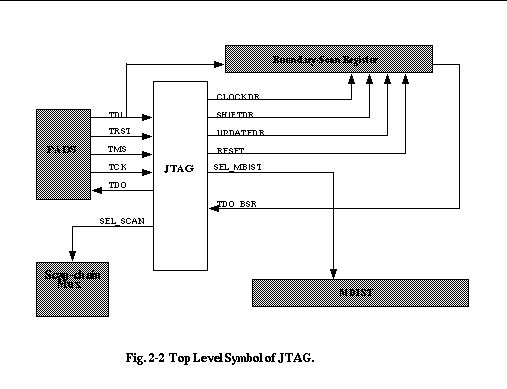
Figure 2-2 shows the logical block diagram. The JTAG consists of one TAP controller and a few registers. There is only one instruction register. The data register can have different number of registers depending on the user requirement.
The TAP is controlled by the Test Clock (TCK) and Test Mode Select (TMS) inputs. These two inputs determine whether an instruction register scan or data register scan is performed.
The TAP consists of a small controller design, driven by the TCK input, which responds to theTMS input as shown in the following state diagram. The IEEE 1149.1 test bus uses both clockedges of TCK. TMS and TDI are sampled on the rising edge of TCK. TDO changes on the falling edge of TCK.
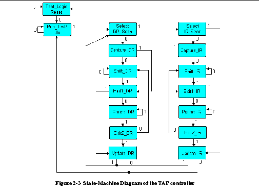
The main state diagram consists of six steady states; Test-Logic-Reset, Run-Test/Idle, Shift-DR, Pause-DR, Shift-IR, and Pause-IR. A unique feature of this protocol is only one steady state exists when TMS is set high: the Test-Logic-Reset state. This means that a reset of the test logic can be achieved within five TCKs or less by setting the TMS input high.
At power up or during normal operation of the host IC, the TAP is forced into the Test-Logic-Reset state by driving TMS high and applying five or more TCKs. In this state, the TAP issues a reset signal placing all test logic in a condition that does not impede normal operation of the host IC. When test access is required, a protocol is applied via the TMS and TCK inputs causing the TAP to exit the Test-Logic-Reset state and move through the appropriate states. From the Run-Test/Idle state, an Instruction Register scan or a Data Register scan can be issued to transition the TAP through the appropriate states shown in the TAP Controller State Diagram above.
The Data and Instruction Register scan states are mirror images of each other, adding symmetry to the protocol sequences.
1) The first action that occurs when either block is entered is a capture operation. For the Data Registers, the Capture-DR state captures (or parallel loads) the data into the selected serial data path. If the BSR is the selected Data Register, the normal data inputs (NDI) is captured during this state. In the Instruction Register, the Capture-IR state captures status information into the Instruction Register.
2) From the Capture state, the TAP transitions to either the Shift or Exit1 state. Normally the Shift state follows the Capture state so that test data or status information can be shifted out for inspection and new data shifted in.
3) Following the Shift state, the TAP either returns to the Run-Test/Idle state via the Exit1 and Update states, or enters the Pause state via Exit1.
4) The Pause state temporarily suspends the data shifting through either the Data or Instruction Register while a required operation, such as refilling a tester memory buffer, is performed.
5) From the Pause state, shifting can resume by re-entering the Shift state via the Exit2 state, or terminate by entering the Run-Test/Idle state via the Exit2 and Update states.
Upon entering the Data or Instruction Register scan blocks, shadow latches in the selected scan path are forced to hold their present state during the Capture and Shift operations. Data shifted into the selected scan path is not output through the shadow latch until the TAP enters the Update-DR or Update-IR state. The Update state causes the shadow latches to update (or parallel load) with the new data that has been shifted into the selected scan path.
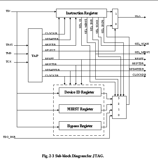
This block consists of one instruction register and several data registers.
The instruction register is responsible for providing the address and control signals required to access a particular data register in the scan path. The instruction register is accessed when the TAP receives an instruction register scan protocol. During an instruction register scan operation the SELECT output from the TAP (Figure 2-2) selects the output of the instruction register to drive the TDO pin. A general instruction register architecture is shown in Figure 2-4. The byte length of the instruction register can be variable depending on how many instructions are needed in an application. For PCNET99, the JTAG instruction byte length is five.
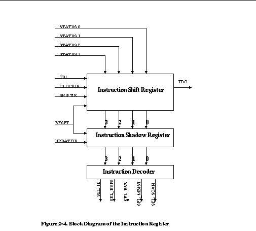
The Instruction Register consists of an instruction shift register and an instruction shadow latch. The instruction shift register (Figure 2-4) consists of a series of shift register bits arranged to form a single scan path between the TDI and TDO pins of the host IC. During Instruction Register scan operations, the TAP exerts control via the Instruction Register shift enable (SHIFTIR) and Instruction Register Clock (CLOCKIR) signals to cause the instruction shift register to preload status information and shift data from TDI to TDO. Both the preload and shift operations occur on the rising edge of TCK; however, the data shifted out from the host IC from TDO occurs on the falling edge of TCK. The status inputs are user-defined observability inputs, except for the two least significant bits, which are always 01 for scan-path testing purposes. (The Instruction Register has a minimum length of two bits.) When activated, the RESET* input sets the instruction shift register to be set to all ones. This forces the device into the functional mode and selects the Bypass Register (or the Device Identification Register if one is present).
The instruction shadow register (Figure 2-4) consists of a series of latches, one latch for each instruction shift register bit. During an Instruction Register scan operation, the latches remain in their present state. At the end of the Instruction Register scan operation, the Instruction Register update (UPDATEIR) input updates the latches with the new instruction installed in the instruction shift register. When activated, the RESET* input sets the latches to all ones.
The IEEE 1149.1 standard requires two Data Registers; Boundary-Scan Register and Bypass Register, with a third, optional, Device Identification Register. This Device ID register is implemented in PCnet99. Additional user-defined MBIST Register is included. The Data Registers are arranged in parallel from the primary TDI input to the primary TDO output. The Instruction Register supplies the address that allows one of the Data Registers to be accessed during a Data Register scan operation. During a Data Register scan operation, the addressed scan register receives TAP control via the Data Register shift enable(SHIFTDR) and Data Register clock (CLOCKDR) inputs to preload test response and shift data from TDI to TDO. During a Data Register scan operation, the SELECT output from the TAP (Figure 2-2) selects the output of the Data Register to drive the TDO pin. When one scan path in the Data Register is being accessed, all other scan paths remain in their present state.
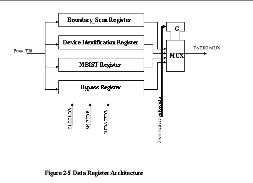
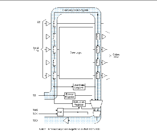
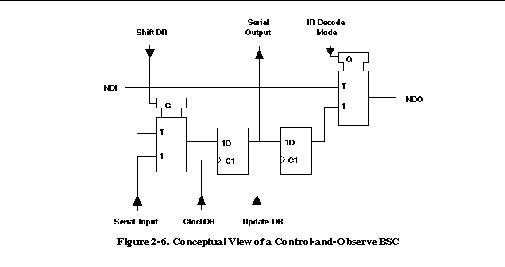
Boundary-Scan Register - The Boundary-Scan Register (BSR) consists of a series of boundary-scan cells (BSCs) arranged to form a scan path around the boundary of the host IC. The BSCs provide the controllability and observability features required to perform boundary-scan testing as described in the Boundary-Scan Overview section of this chapter. Shadow latches in the BSCs, driving the NDO outputs remain in their present state during a Data Register scan operation. At the end of a Data Register scan operation, the Data Register update (UPDATEDR) input updates the shadow latches with the new boundary test pattern to be applied from the NDO outputs of the BSCs. Figure 2-6 shows a conceptual view of a Control-and-Observe BSC.
Bypass Register - The Bypass Register consists of a single scan register bit. When selected, the Bypass Register provides a single bit scan path between TDI and TDO. The Bypass Register allows abbreviating the scan path through devices that are not involved in the test. The Bypass Register is selected when the Instruction Register is loaded with a pattern of all ones to satisfy the IEEE 1149.1 Bypass instruction requirement.
Device Identification Register - The Device Identification Register is an optional register defined by IEEE 1149.1, to identify the device's manufacturer, part number, revision, and other device-specific information. Figure 2-7 shows the bit assignments defined for the Device Identification Register. These bits can be scanned out of the Identification Register after being selected.
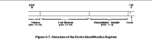
Although the Device Identification Register is optional, IEEE 1149.1 specification has dedicated an instruction to select this register. The Device Identification Register is selected when the Instruction Register is loaded with the IDCODE instruction, which is defined by the vendor.
Manufacturer's identification codes (Bit1 through Bit11) are assigned, maintained, and updated by the EIA/JEDEC office. Any company can be added to the JEDEC Standard Manufacturer's Identification Code (Publication JEP106) by request to the JEDEC office at 202-457-4973.
SEL_MBIST - This signal will be asserted when the current JTAG instruction is MBIST. It is the enable signal for running BIST test.
SEL_SCAN - This signal will be asserted when the current JTAG instruction is SCANTEST. It is the multiplexer select signal for ATPG scan-chain related pins.
The IEEE 1149.1 standard defines nine test instructions. Three of them are required. The following subsections contain brief descriptions of each required test instruction.
BYPASS Instruction (Instruction Code: 1111)
The required BYPASS instruction allows the IC to remain in a functional mode and selects the Bypass Register to be connected between TDI and TDO. The BYPASS instruction allows serial data to be transferred through the IC from TDI to TDO without affecting the operation of the IC. The bit code of this instruction is defined to be all ones by the IEEE 1149.1 standard.
SAMPLE/PRELOAD Instruction (Instruction Code: 0001)
The required SAMPLE/PRELOAD instruction allows the IC to remain in its functional mode and selects the Boundary-Scan Register to be connected between TDI and TDO. During this instruction, the Boundary-Scan Register can be accessed via a data scan operation, to take a sample of the functional data entering and leaving the IC. This instruction is also used to preload test data into the Boundary-Scan Register prior to loading an EXTEST instruction. The bit code for this instruction is defined by the user.
EXTEST Instruction (Instruction Code: 0000)
The required EXTEST instruction places the IC into an external boundary test mode and selects the Boundary-Scan Register to be connected between TDI and TDO. During this instruction, the Boundary-Scan Register is accessed to drive test data off-chip via the boundary outputs and receive test data off-chip via the boundary inputs. The bit code of this instruction is defined by the 1149.1 standard to be all zeros.
INTEST Instruction (Instruction Code: 0010)
The optional INTEST instruction places the IC in an internal boundary test mode and selects the Boundary-Scan Register to be connected between TDI and TDO. During this instruction, the Boundary-Scan Register is accessed to drive test data on-chip via the boundary inputs and receive test data on-chip via the boundary outputs. The bit code of this instruction is defined by the user.
MBIST Instruction (Instruction Code: 0100)
The optional MBIST instruction places the IC into a self-test mode, enables a comprehensive self-test of the IC's core logic, and selects a user-specified Data Register to be connected between TDI and TDO. During this instruction, the boundary outputs are controlled so that they cannot interfere with neighboring ICs during the MBIST operation. Also, the boundary inputs are controlled so that external signals cannot interfere with the MBIST operation. The bit code of this instruction is defined by the user.
IDCODE Instruction (Instruction Code: 1000)
The optional IDCODE instruction allows the IC to remain in its functional mode and selects an optional Device Identification Register to be connected between TDI and TDO. The Identification Register (see Figure 3-8) is a 32-bit shift register containing information regarding the IC manufacturer, device type, and version code. Accessing the Identification Register does not interfere with the operation of the IC. Also, access to the Identification Register should be immediately available, via a TAP data scan operation, after power-up of the IC or after the TAP has been resetusing the optional TRST* pin or by issuing a Test-Logic-Reset instruction. The bit code of this instruction is defined by the IC device designer.
SCANTEST Instruction (Instruction Code: 0111)
The optional SCANTEST instruction places the IC in an scan-chain test mode and selects the Bypass Register to be connected between TDI and TDO. During this instruction, the JTAG logic is idled, and the scan-chain related pins (i.e. SCLK, SI, SO and SE pins) are multiplexed to the input and output pads. The user can perform a ATPG scan without caring about the JTAG block. The bit code of this instruction is defined by the user.